

Analysis & Optimization of Sense Amplifierfor Deep Sub-micron SRAM
Nguyen Le Minh Hoang
Le Bao Duy
Nguyen Hai Quyen
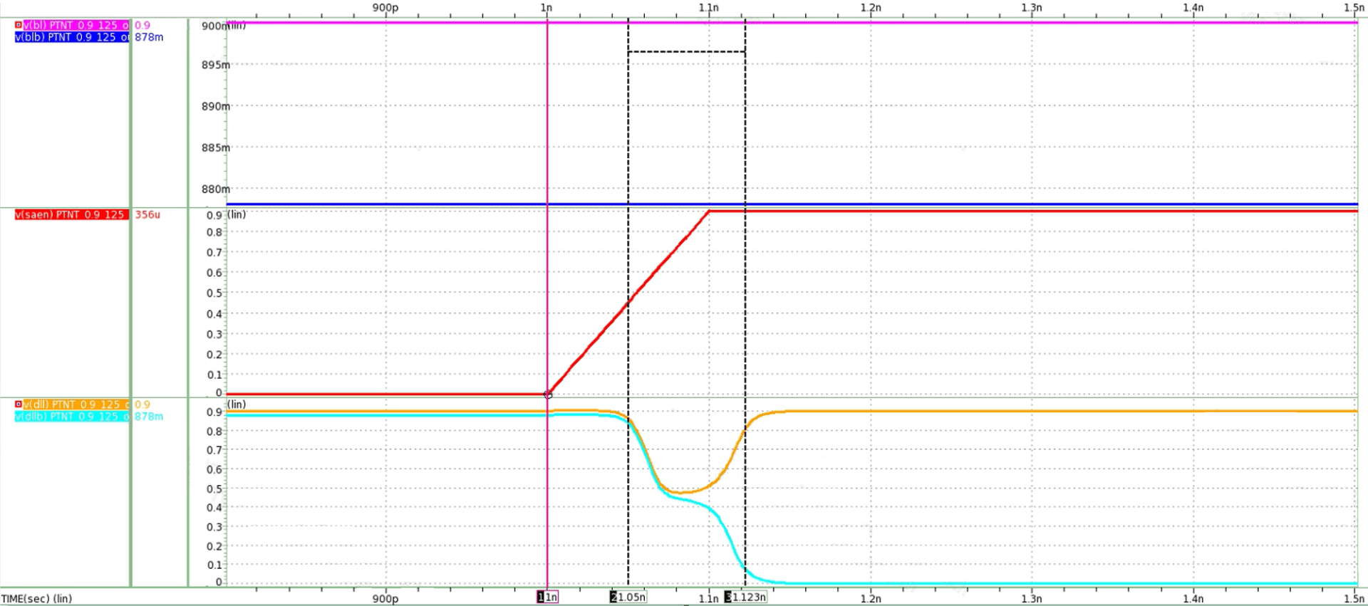
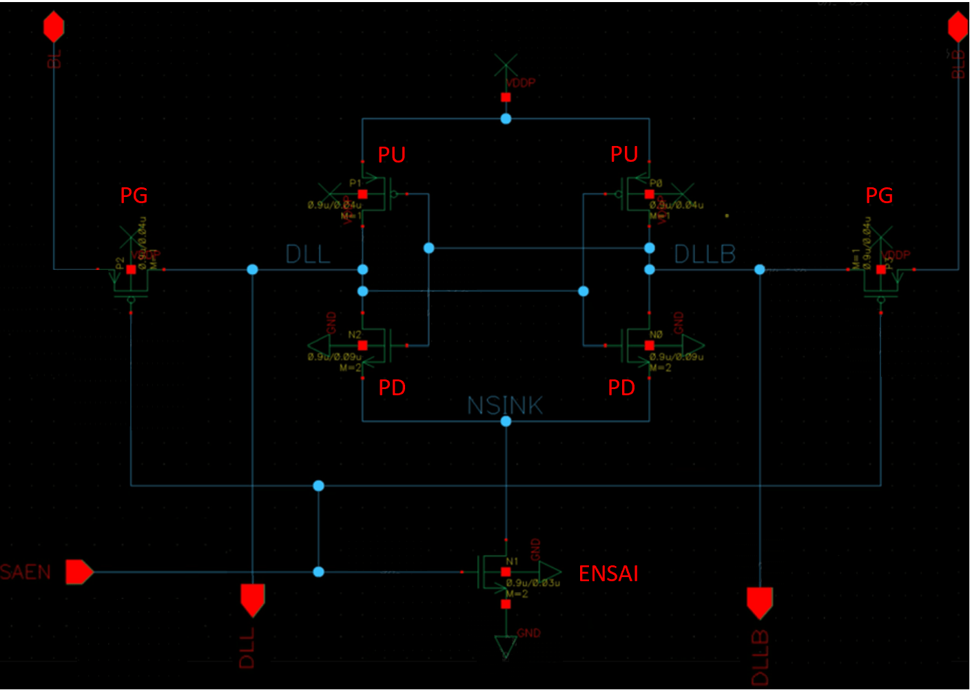
As technology node shrinks, variation effects during fabrication are a major issue that can lead to the failure of the functional Intellectual Property (IP) blocks in System on a Chip. In Memory Intellectual Property block especially Static Random Access Memory (SRAM), this is an issue due to variation in Delta V (the differential voltage between bit-lines) of the Sense Amplifier (SA). Sense Amplifier is the most important peripheral circuit in the SRAM memory, which is used to amplify the Delta V in the read operation of the SRAM and create full swing digital output signal.
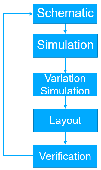
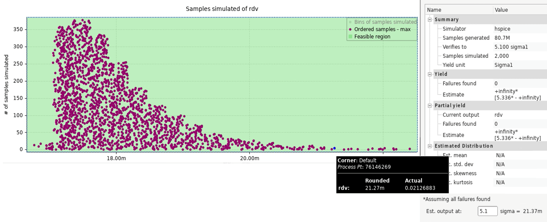
In this project, we are working under the supervision of Faraday Vietnam to focus on designing and testing the Latch Sense Amplifier of the SRAM using the 22nm technology node. The main target of this project is to investigate all the factors that affect Delta V, optimize the circuit and layout design to evaluate and then minimize negative factors. The design process will include several circuit and layout techniques such as High Sigma Monte Carlo prediction, Common-Centroid layout technique, and Resistor/Capacitor (RC) balancing evaluation method, etc.
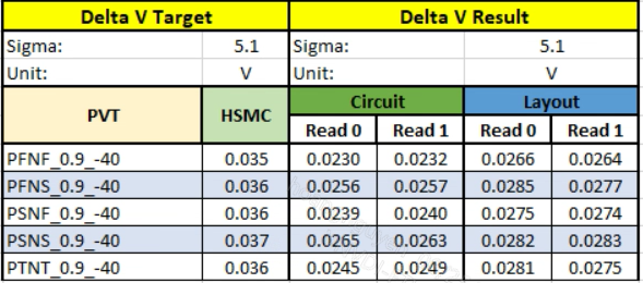
Our design need to fulfil the specific design targets provided by Faraday, which are Minimum Delta V and Sense Time values at various process corners, supply voltages, and operating temperatures. For circuit design, our targets are achieving the target minimum Delta V (to ensure correct read output), Sense Time (to have better read speed), and high manufacturing yield (to reduce chip defects). For layout design, the targets are achieving best R/C balancing (to reduce circuit parasites), targeted minimum Delta V, Sense Time values, and minimizing crosstalk effect (to reduce delays and noises).

Demo Video