Design of CMOS Phase-Locked Loop
The inexorable march toward 6G—the next frontier in wireless communication—brings with it both promise and challenge. As we aim for data rates surpassing those of 5G, the sub-terahertz (sub-THz) frequency bands emerge as the playground for innovation. These bands, particularly the W and D bands, hold potential for CMOS-based mobile transceivers. However, a formidable obstacle looms: the generation of local-oscillation (LO) signals with ultra-low jitter. Jitter, the temporal variation in signal edges, directly impacts the error vector magnitude (EVM) of transmitted signals. In the sub-THz regime, achieving EVM targets necessitates reducing the root mean square (RMS) jitter to well below 100 femtoseconds (fs). While the cascade architecture has traditionally been employed for sub-THz LO signal generation, its hunger for power and silicon area prompts exploration of more efficient alternatives. Enter the single-stage phase-locked loop (PLL), a compact solution that promises improved power utilization. However, the delicate balance between loop bandwidth and noise suppression remains a critical challenge. To address this, the subsampling PLL (SSPLL) emerges as a potential savior. By harnessing the inherent sampling gain of the subsampling phase detector (SSPD), the SSPLL seeks to reconcile jitter reduction with power efficiency. Our project embarks on this intricate journey, reviewing existing topologies and designing a sub-THz PLL that treads the fine line between performance and practicality.
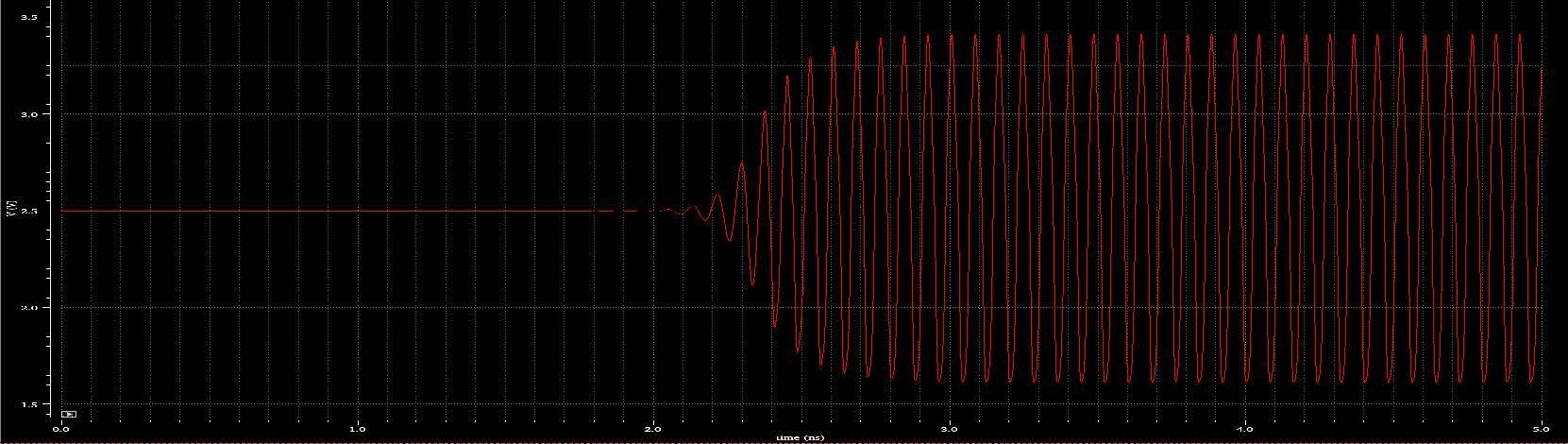
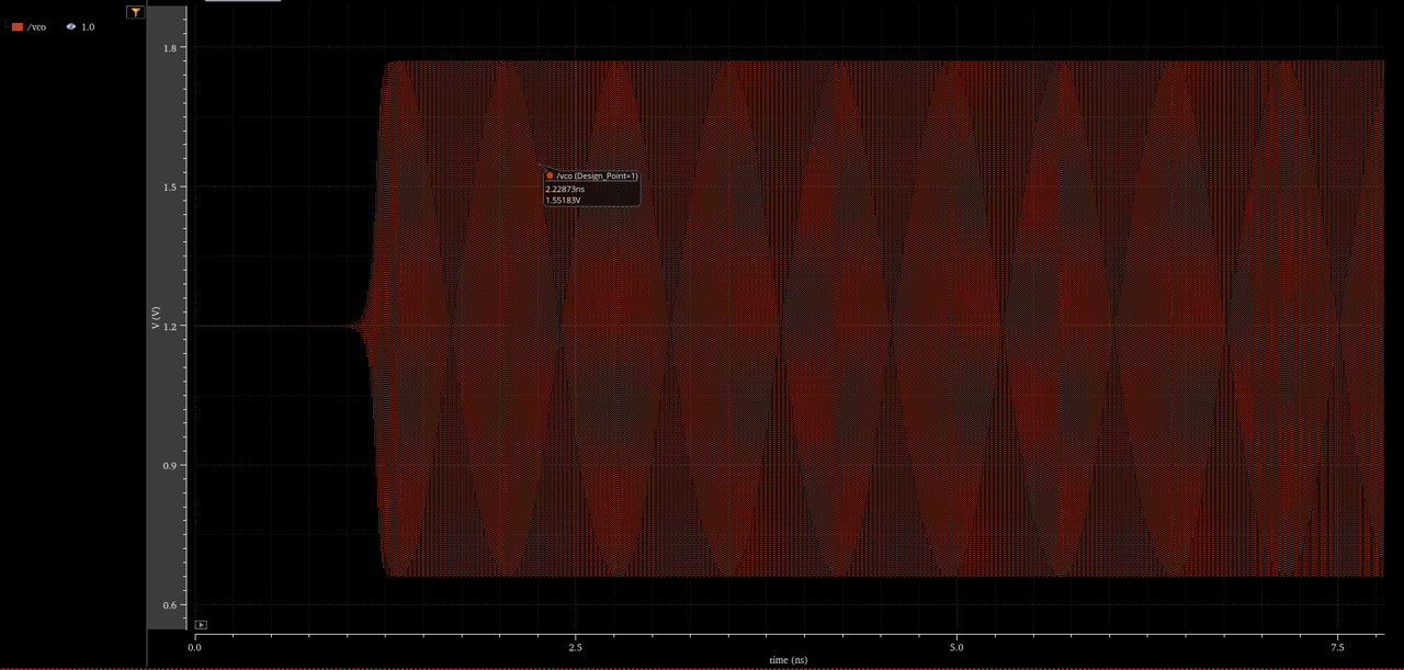
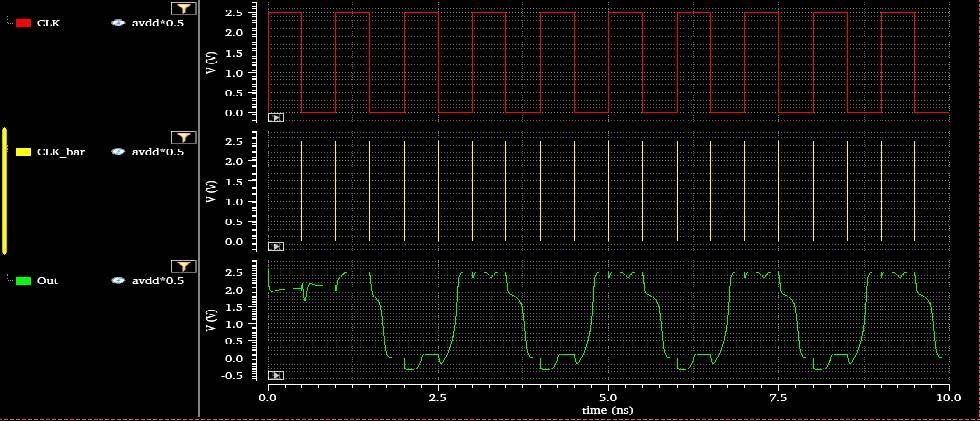
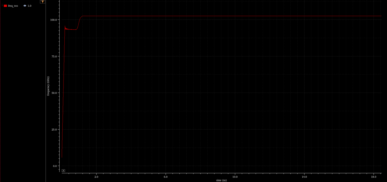
Project Snapshots